Complete electronic board component population utilizing modern assembly pipelines for zero-defect component integration.
A raw, fabricated printed circuit board is simply a roadmap of copper traces. It only gains intelligence when components are physically integrated onto its surface. PCB Assembly (PCBA) is the highly complex process of populating microprocessors, passives, connectors, and ball grid arrays onto bare boards with flawless mechanical accuracy.
Modern electronic assembly demands precision down to the micron level. As consumer tech shrinks and industrial platforms grow more dense, surface mount technology (SMT) has surpassed manual human capabilities. Utilizing automated high-speed component mounting systems combined with explicit solder paste deposit profiles ensures that your hardware runs reliably without internal connectivity failure.
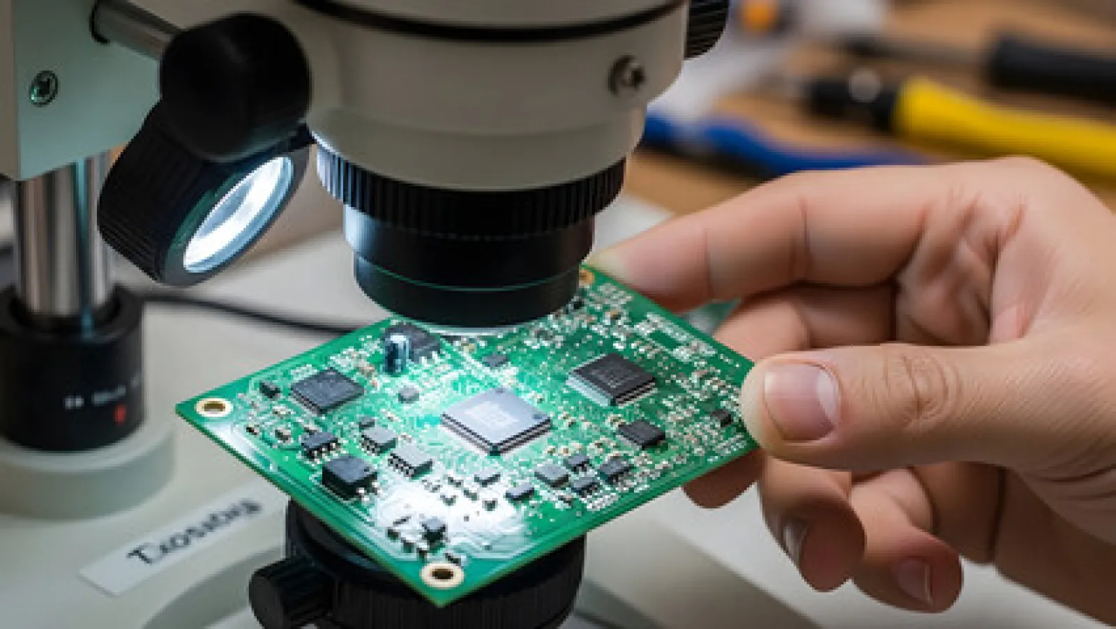
Automated Line Operation
SMT placement running real-time placement verification.
Managing stencil apertures, reflow cycles, and automated optical validation loops.
The core challenge of automated assembly sits inside the multi-zone reflow oven. Solder paste is a precise mixture of microscopic metal spheres and chemical flux. If a board heats up too quickly, the flux boils unevenly, shifting passive components into an upright defect state known as "tombstoning." If it cools too slowly, the copper joints become brittle, cracking easily under industrial vibration.
To guarantee zero-defect boards, we carefully monitor the unique thermal envelope of every single assembly run. We optimize stencil apertures using laser-cut nickel structures, and deploy advanced Automated Optical Inspection (AOI) scanners along with micro-focus X-ray systems to instantly verify inner-layer solder connections under fine-pitch Ball Grid Arrays (BGAs).
"High-yield component populating relies directly on Design for Assembly (DFA) compliance. Thermal distribution properties across large copper pads must match miniature trace layouts perfectly to prevent structural wetting faults."
— Factory Surface Mount Engineering Audit
Sourcing individual components internationally splits your bills of materials across multiple vendors, leaving you vulnerable to hidden brokerage fees, custom hold-ups, and counterfeits.
At pcbmadeinindia.com, our local procurement channels take full ownership of component logistics. We work directly with verified domestic franchises and global global suppliers to clear parts through a single, trace-audited intake cycle.
By coordinating your fabrication and component assembly under a single regional framework, you eliminate the risk of parts not fitting bare-board dimensions.
Our local engineering group runs simultaneous Design for Assembly (DFA) checks on your component packages. If a component footprint conflicts with actual manufacturer specs, we address the issue directly with your team locally, skipping the long communication delays of overseas assembly providers.
Granular parameter limits for our automated SMT and manual through-hole lines.
| Assembly Attribute | Standard Line Range | Advanced System Limits |
|---|---|---|
| Assembly Types Supported | Single or Double-Sided SMT / Through-Hole | Mixed Complex Turnkey / Flex Placements |
| Minimum Passive Footprint | 0402 Packages | 0201 Ultra-Miniature Packages |
| BGA Pitch Capabilities | 0.5mm Fine Pitch | Down to 0.4mm with X-Ray Verification |
| Solder Chemistry Selection | Standard Leaded (Sn63/Pb37) | Lead-Free RoHS Compliant (SAC305) |
| Max Panel Dimensions | 400mm x 350mm | Up to 510mm x 460mm Large Boards |
| Post-Assembly Diagnostics | Visual Inspection + Automated 3D AOI | In-Circuit Testing (ICT) / Functional Testing |
Note: Functional testing setups require custom programming guides, firmwares, and explicit terminal validation test fixtures supplied by the customer.
Streamline your electronic assembly workflow. Upload your Gerber files along with your Bill of Materials (BOM) today for an immediate, unified turnkey production analysis.