Advanced schematic validation and trace optimization crafted specifically to ensure smooth manufacturing integration.
A schematic diagram represents the conceptual logic of an electronic circuit, but the physical layout determines whether that circuit functions in the real world. PCB design is the meticulous engineering discipline of translating abstract nets and components into physical copper pathways, balancing electromagnetic fields, thermal distribution, and manufacturing tolerances.
As modern ICs operate at higher frequencies and lower voltages, traces can no longer be treated as simple connections. They behave as transmission lines. Poorly optimized trace routing introduces parasitic capacitance, ground bounce, and signal distortions that destroy prototype yields. High-speed hardware demands predictive, rule-driven layout architecture before a single panel ever hits the fabrication floor.
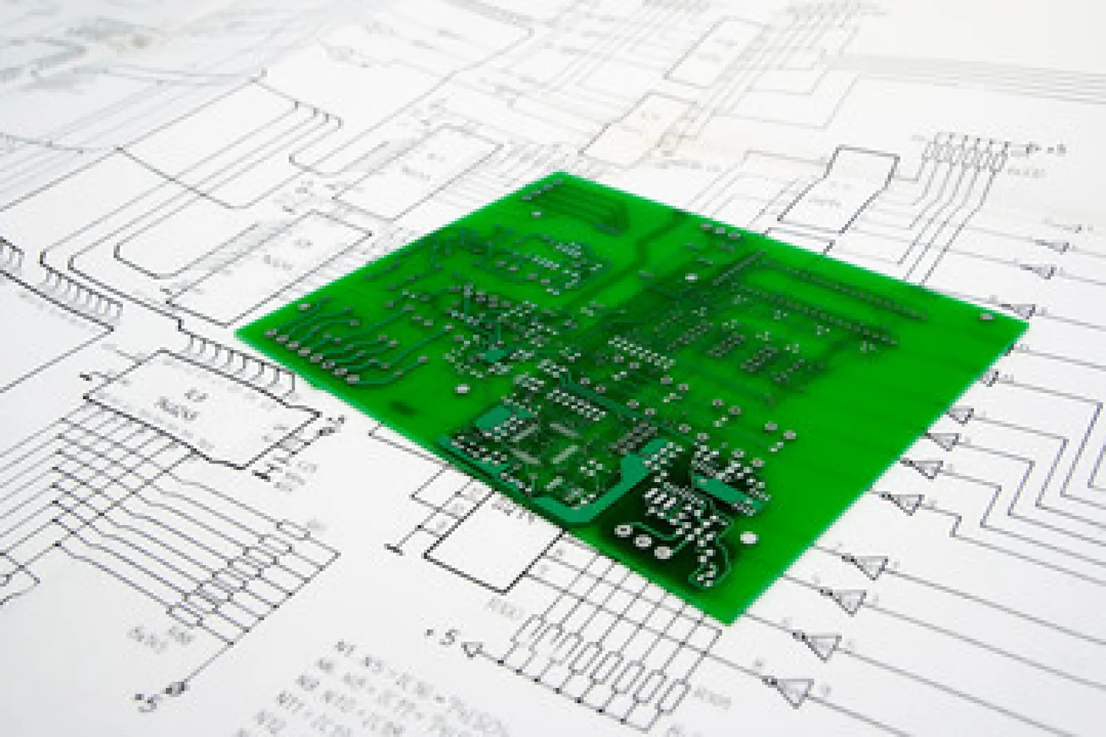
CAD Signal Topography
Multi-tier propagation constraints modeling inside high-speed routing engines.
Mitigating cross-talk, managing return paths, and optimizing plane stackups.
When clock signals execute transitions at sub-nanosecond speeds, adjacent traces can unintentionally couple with one another, a destructive electromagnetic phenomenon known as cross-talk. To preserve signal integrity, our design process isolates high-speed buses from sensitive analog tracking zones using robust ground shielding, continuous return paths, and strict length-matching rules for differential pairs.
Thermal management is equally tied to track layout choices. High-current power rails require dense copper fill zones and arrays of carefully placed thermal vias to pass heat away from processing chips into inner power planes. By performing upfront multi-layer stackup planning, we control structural impedance lines natively, matching substrate constants to your explicit application.
"A schematic captures an engineer's design intent, but the board layout dictates its operational reality. Minor errors in component placement or ground plane distribution will alter circuit characteristics permanently."
— Systems Engineering Layout Standard
Outsourcing layout services to isolated agencies often results in designs that look flawless on screen but fail basic physical manufacturing rules.
At pcbmadeinindia.com, our design desk is directly connected to our local fabrication facility. We implement real-time **Design for Manufacturability (DFM)** and Design for Assembly (DFA) rules right during layout drafting, ensuring your project sails smoothly into manufacturing with no rework.
We eliminate the typical friction between layout designers and factory manufacturing groups. By keeping your design engineering local, we provide transparent support that honors your precise application goals.
Our layout engineers evaluate your circuit structures locally, checking everything from pad layout geometry to mechanical stackup clearance definitions. This localized, human-crafted engineering framework protects your project from expensive mistakes and logistics gaps, ensuring your product is optimized for production from day one.
Granular parameter limits and platform coverage for our layout engineering desk.
| Design Attribute | Standard Offering | Advanced Parameters |
|---|---|---|
| Layer Constraints | 1 to 4 Layers Rigid Layouts | Up to 12 Layers / Rigid-Flex Arrays |
| High-Speed Bus Interfaces | SPI, I2C, Standard USB 2.0 / 3.0 Traces | DDR3/DDR4, PCIe Gen3, Impedance Matched HDMI |
| Minimum Trace / Space Rules | 6 mil (0.15mm) Trace Pathing | Down to 4 mil (0.1mm) Dense High-Speed Layouts |
| Supported EDA Toolchains | KiCad, Autodesk Eagle Systems | Altium Designer, OrCAD / Allegro Layout Engine |
| Design Integrity Verification | Standard Schematic DRC Matching | Signal Cross-talk Analysis & Component Collision Checks |
| Engineering Deliverables | Standard Gerber RS-274X Formats | Production IPC-2581 / ODB++ Databases + Complete BOM Files |
Note: Schematic conversions from obsolete toolchains or recovery from scanned paper graphics require direct technical validation before engineering kickoff.
Stop battling complex design constraints alone. Share your schematic files with our layout engineering group for an in-depth stackup analysis and professional routing consultation today.